×


Cypress公司的S6BP501A/S6BP502A是三路输出功率管理集成电路,包括一个高压降压DC/DC控制器(DD3V),一个内置了FET的降压DC/DC转换器(DD1V)和一个内置了FET的升压DC/DC转换器(DD5V);电流模式架构具有快速负载响应特性,无负载时输入电流降至15 μA,输入电压宽至2.5V-42V,和AEC-Q100 (Grade-2)兼容.主要用在仪表盘,汽车电子和工业应用.本文介绍了S6BP501A/S6BP502A主要特性,框图和架构图,应用电路及其所用材料清单,以及评估板S6SBP501A00VA1001和S6SBP502A00VA1001主要指标,框图,电路图,材料清单和PCB设计图.
S6BP501A/S6BP502A is a three channel output power management IC. This IC includes one high voltage buck DC/DC controller(DD3V), one buck DC/DC converter with built-in FETs (DD1V) and one boost DC/DC converter with built-in FETs (DD5V). Currentmode architecture is used for fast load transient response. At no load, the input supply current is reduced to 15 μA (Typ). It is possibleto provide stable output voltage under an automotive cold cranking condition until the input voltage falls to 2.5V. This IC is suitable forpower supply solutions of automotive and Industrial applications. Each output voltage can be adjusted by external resistors. BothDD1V and DD5V support the switching frequencies up to 2.4 MHz to allow use of small size inductors, which can reduce a partmounting area. To decrease EMI, this IC equips a SYNC function that synchronizes to an external clock signal and a spread spectrumclock generator (SSCG). When not inputting an external clock, it operates by an internal clock. The SSCG is valid both internal clockand external clock. Moreover, this IC has power good (PG) monitors for each output and a thermal-warning indicator.
S6BP501A/S6BP502A主要特性:
Wide input voltage range : 2.5V to 42V (DD3V)
Adjustable output voltage with pairs of resistors
DD1V : 1.0V to 1.3V
DD3V : 3.2V to 3.4V
DD5V : 5.0V to 5.2V
Switching frequency range (synchronizable to external clockby SYNC function)
DD1V, DD5V
Internal clock operation : 2.1 MHz (Typ)
External clock operation : 1.8 MHz to 2.4 MHz
DD3V (one-fifth-divided clock)
Internal clock operation : 420 kHz (Typ)
External clock operation : 360 kHz to 480 kHz
Super-high efficiency by PFM operation (DD3V, DD5V :
When fixing SYNC pin to a low level)
Automatic PWM/PFM switching and fixed PWM operationsare settable by SYNC pin (DD3V, DD5V)
Operable on up to 100% duty (DD3V)
Built-in phase compensators
Built-in SSCG(spread spectrum clock generator)
Synchronous rectification current mode architecture
Shutdown current : 1 μA (Typ)
Quiescent current : 15 μA (Typ)
Load-independent soft-start
Power good monitors for each output
OVD (over voltage detection)
UVD (under voltage detection)
Enhanced protection functions
UVLO (under voltage lockout)
OVP (over voltage protection)
OCP (over current protection)
TSD (thermal shutdown)
TWI (thermal warning indicator)
Wettable QFN-32 package : 5 mm × 5 mm
AEC-Q100 compliant (Grade-2)
S6BP501A/S6BP502A应用:
Instrument cluster
Automotive applications
Industrial applications
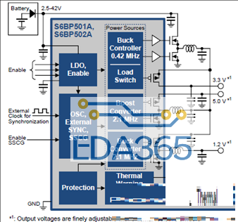
图1.S6BP501A/S6BP502A框图

图2.S6BP501A/S6BP502A架构图
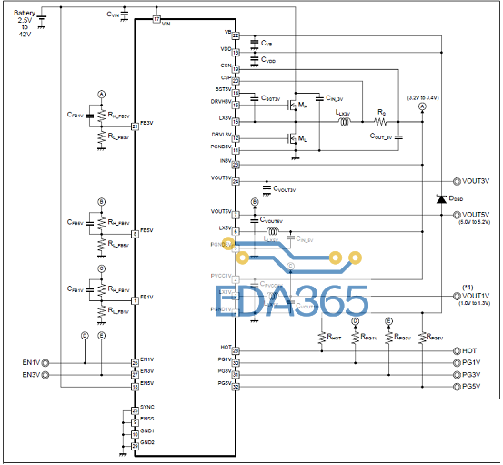
图3.S6BP501A/S6BP502A应用电路
图3S6BP501A/S6BP502A应用电路材料清单:

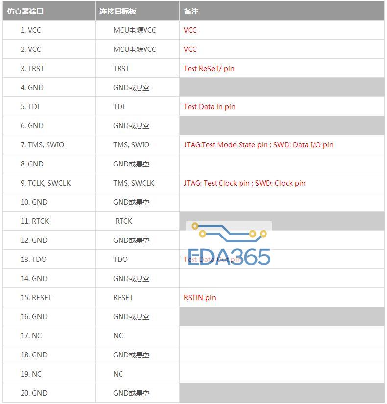
评估板S6SBP501A00VA1001和S6SBP502A00VA1001
S6SBP501A00VA1001 and S6SBP502A00VA1001 are evaluation kits for the power block of an automotive instrumentcluster. These boards implement the Cypress power management IC S6BP501A and S6BP502A respectively.
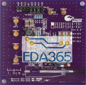
图4.评估板S6SBP501A00VA1001和S6SBP502A00VA1001外形图
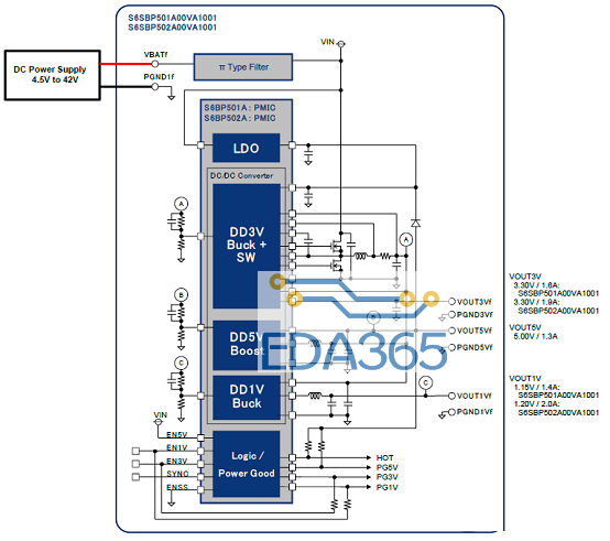
图5.评估板S6SBP501A00VA1001和S6SBP502A00VA1001框图
评估板S6SBP501A00VA1001和S6SBP502A00VA1001主要指标:
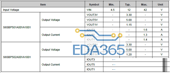
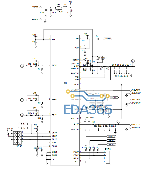
图6.评估板S6SBP501A00VA1001和S6SBP502A00VA1001电路图
评估板S6SBP501A00VA1001和S6SBP502A00VA1001材料清单:
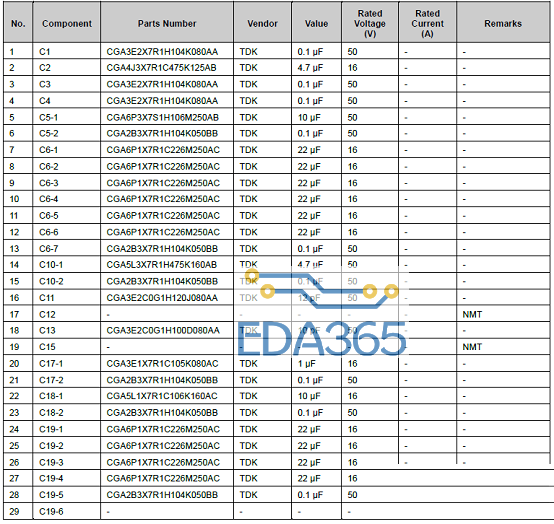
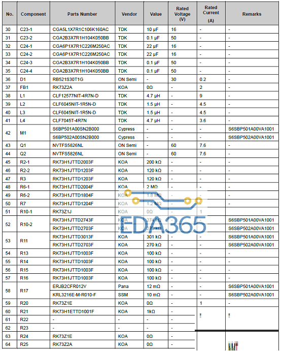
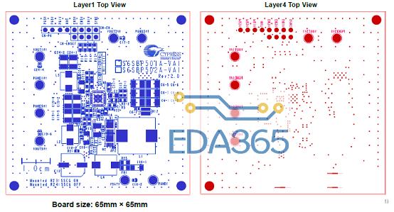
图7.评估板S6SBP501A00VA1001和S6SBP502A00VA1001 PCB设计图(1)
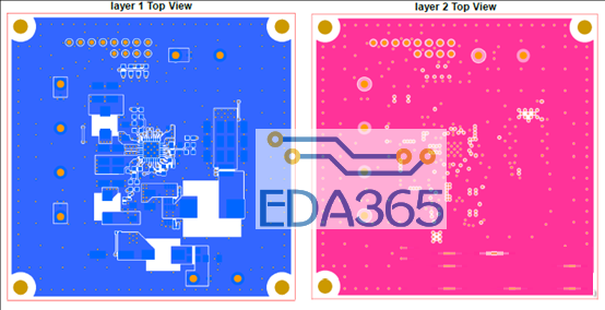
图8.评估板S6SBP501A00VA1001和S6SBP502A00VA1001 PCB设计图(2)
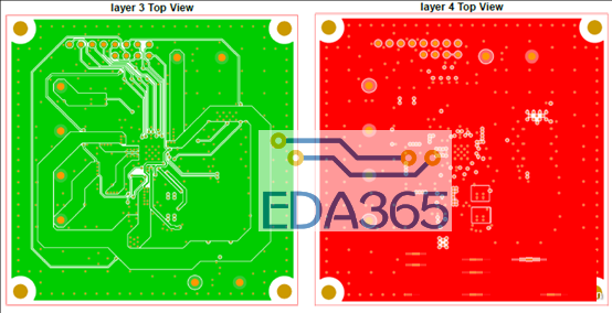
图9.评估板S6SBP501A00VA1001和S6SBP502A00VA1001 PCB设计图(3)
『本文转载自网络,版权归原作者所有,如有侵权请联系删除』


 热门文章
更多
热门文章
更多

 车联网[号角"已吹响 但技术落地仍待市场考验


 APP下载
APP下载 登录
登录


