×


Cypress公司的S6E2G系列是32位Arm® Cortex®-M4F FM4微控制器,CPU工作频率高达180MHz,集成了1MB闪存,192KB SRAM,20x通信外设,33x数字外设和3x模拟外设,具有高性能和有竞争力的成本,设计用于工业自动化和测试测量。本文介绍了S6E2G系列主要特性和产品详细特性,框图,以及两种版本开发平台FM4-U120-9B560主要特性和电路图。
FM4-U120-9B560 - Arm® Cortex®-M4 MCU Starter Kit with USB and CMSIS-DAP S6E2G Series are FM4 devices with up to 180 MHz CPU, 1 MB flash, 192 KB SRAM, 20x communication peripherals, 33x digitalperipherals and 3x analog peripherals. They are designed for industrial automation and metering applications.
Devices in the S6E2G Series are highly integrated 32-bit microcontrollers with high performance and competitive cost. This series isbased on the Arm® Cortex®-M4F processor with on-chip flash memory and SRAM. The series has peripherals such as motor controltimers, A/D converters, and communications interfaces (USB, CAN, UART, CSIO (SPI), I2C, LIN)。
S6E2G系列主要特性:
32-bit Arm Cortex-M4F Core
Up to 180 MHz frequency operation
On-chip Memories
Flash memory: Up to 1024 Kbytes
SRAM memory:
• SRAM0: up to 128 Kbytes
• SRAM1: 32 Kbytes
• SRAM2: 32 Kbytes
Direct Memory Access (DMA) Controller (Eight Channels)
Descriptor System Data Transfer Controller (DSTC);256 channels
External Bus Interface
USB Interface (Max two channels): Host and Device
CAN Interface (Max one channel) Available on S6E2GMand S6E2GH Devices Only
Multi-function Serial Interface (Max 10 Channels)
UART (Universal Asynchronous Receiver/Transmitter)
Clock Synchronous Serial Interface (CSIO (SPI))
Local Interconnect Network (LIN)
Inter-Integrated Circuit (I2C)
Inter-IC Sound (I2S)
Base Timer (Max 16 channels)
General Purpose I/O Port
Up to 121 high-speed general-purpose I/O ports in 144-pinpackage
Up to 153 high-speed general-purpose I/O ports in 176-pinpackage
Multi-function Timer (Max two units)
Real-Time Clock (RTC)
Analog to Digital Converter (ADC) (Max 32 Channels)
Dual Timer (32-/16-bit Down Counter)
Quadrature Position/Revolution Counter (QPRC; Max twochannels)
Watch Counter
External Interrupt Controller Unit
Watchdog Timer (Two channels)
Cyclic Redundancy Check (CRC) Accelerator
SD Card Interface Available on S6E2GM, S6E2GH, andS6E2GK Devices Only
Ethernet-MAC Available on S6E2GM, S6E2GK, andS6E2G2 Devices only
Smartcard Interface (Max 2 channels)
Five Clock Sources
Six Reset Sources
Clock Supervisor (CSV)
Low-Voltage Detector (LVD)
Six Low-power Consumption Modes
Sleep
Timer
RTC
Stop
Deep standby RTC
Deep standby stop
Peripheral Clock Gating System
Crypto Assist Function
Debug
Serial wire JTAG debug port (SWJ-DP)
Embedded trace macrocells (ETM) provide comprehensivedebug and trace facilities.
AHB trace macrocells (HTM)
41-bit Unique ID
Wide range voltage: VCC = 2.7 to 5.5 V
图1. S6E2G系列框图
S6E2G系列产品详细特性:
32-bit Arm Cortex-M4F Core
Up to 180 MHz frequency operation
FPU built-in
Support DSP instructions
Memory protection unit (MPU): improves the reliability of anembedded system
Integrated nested vectored interrupt controller (NVIC): 1NMI (non-maskable interrupt) and 128 peripheral interruptsand 16 priority levels
24-bit system timer (Sys Tick): system timer for OS taskmanagement
On-chip Memories
Flash memory
This series is on-chip flash memories.
Up to 1024 Kbytes
Built-in flash accelerator for zero wait state
Security function for code protection
SRAM
This is composed of three independent SRAMs (SRAM0,SRAM1 and SRAM2)。 SRAM0 is connected to the I-code busand D-code bus of Cortex-M4F core. SRAM1 and SRAM2
are connected to system bus of Cortex-M4F core.
SRAM0: up to 128 Kbytes
SRAM1: 32 Kbytes
SRAM2: 32 Kbytes
External Bus Interface
Supports SRAM, NOR, NAND flash and SDRAM device
Up to 9 chip selects CS0 to CS8 (CS8 is only for SDRAM)
8-/16-/32-bit data width
Up to 25-bit address bus
Supports address/data multiplexing
Supports external RDY function
Supports scramble function
Possible to set the validity/invalidity of the scramblefunction for the external areas 0x6000_0000 to0xDFFF_FFFF in 4 Mbytes units.
Possible to set two kinds of the scramble key
USB Interface (Max two channels)
The USB interface is composed of a Device and a Host.
USB Device
USB 2.0 Full-speed supported
Max 6 EndPoint supported
• EndPoint 0 is control transfer
• EndPoint 1,2 can be selected bulk-transfer, interrupttransferor isochronous-transfer
• EndPoint 3 to 5 can select bulk-transfer or interrupttransfer
EndPoint 1 to 5 comprise double buffer
The size of each endpoint is as follows.
• Endpoint 0, 2 to 5: 64 byte
• EndPoint 1: 256 byte
USB Host
USB2.0 Full-Speed/Low-Speed supported
Bulk-transfer, interrupt-transfer, and isochronoustransfersupport
USB Device connected/dis-connected automaticallydetect
IN/OUT token handshake packet automatically
Max 256-byte packet length supported
Wake-up function supported
CAN Interface (Max one channel) Available onS6E2GM and S6E2GH Devices Only
Compatible with CAN specification 2.0A/B
Maximum transfer rate: 1 Mbps
Built-in 32-message buffer
Multi-function Serial Interface (Max 10 Channels)
Separate 64 byte receive and transmit FIFO buffers forchannels 1 and channels 4 to 7.
Operation mode is selectable for each channel from thefollowing:
UART
CSIO (SPI)
LIN
I2C
I2S
UART
Full-duplex double buffer
Selection with or without parity supported
Built-in dedicated baud rate generator
External clock available as a serial clock
Various error detect functions available (parity errors,framing errors, and overrun errors)
CSIO (SPI)
Full-duplex double buffer
Built-in dedicated baud rate generator
Overrun error detect function available
Serial chip select function (ch 6 and ch 7 only)
Supports high-speed SPI (ch 4 and ch 6 only)
Data length 5 to 16-bit
LIN
LIN protocol Rev.2.1 supported
Full-duplex double buffer
Master/slave mode supported
LIN break field generation (can change to 13- to 16-bitlength)
LIN break delimiter generation (can change to 1- to 4-bitlength)
Various error detect functions available (parity errors,framing errors, and overrun errors)
I2C
Standard mode (Max 100 kbps)/Fast mode (Max 400 kbps)supported
Fast mode Plus (Fm+) (Max 1000 kbps, only for ch 3 = ch Aand ch 7 = ch B) supported
I2S
Using CSIO (SPI) (ch 1 only) and I2S clock generator
Supports two transfer protocol: I2S and MSB-justified
Master mode only
DMA Controller (Eight Channels)
DMA controller has an independent bus, so the CPU andDMA controller can process simultaneously.
Eight independently configured and operated channels
Transfer can be started by software or request from thebuilt-in peripherals
Transfer address area: 32-bit (4 GB)
Transfer mode: Block transfer/Burst transfer/Demandtransfer
Transfer data type: bytes/half-word/word
Transfer block count: 1 to 16
Number of transfers: 1 to 65536
DSTC (Descriptor System Data Transfer Controller;256 channels)
The DSTC can transfer data at high-speed without going viathe CPU. The DSTC adopts the descriptor system and,following the specified contents of the descriptor that has
already been constructed on the memory, can access directlythe memory/peripheral device and perform the data-transferoperation.
It supports the software activation, the hardware activation,and the chain activation functions.
A/D Converter (Max 32 Channels)
12-bit A/D Converter
Successive approximation type
Built-in three units
Conversion time: 0.5 μs at 5 V
Priority conversion available (priority at two levels)
Scanning conversion mode
Built-in FIFO for conversion data storage (for SCANconversion: 16 steps, for priority conversion: 4 steps)
Base Timer (Max 16 channels)
Operation mode is selected from the following for eachchannel:
16-bit PWM timer
16-bit PPG timer
16-/32-bit reload timer
16-/32-bit PWC timer
Event counter mode (External clock mode)
General Purpose I/O Port
This series can use its pins as general purpose I/O portswhen they are not used for external bus or peripherals;moreover, the port relocate function is built in. It can set the
I/O port to which the peripheral function can be allocated.
Capable of pull-up control per pin
Capable of reading pin level directly
Built-in port-relocate function
Up to 121 high-speed general-purpose I/O ports in 144-pinpackage
Some pins 5 V tolerant I/O.
See 6. Pin Descriptions and 7. I/O Circuit Type for thecorresponding pins.
Multi-function Timer (Max two units)
The multi-function timer is composed of the following blocks:Minimum resolution: 5.56 ns
16-bit free-run timer × 3 ch/unit
Input capture × 4 ch/unit
Output compare × 6 ch/unit
A/D activation compare × 6 ch/unit
Waveform generator × 3 ch/unit
16-bit PPG timer × 3 ch/unit
The following functions can be used to achieve the motorcontrol:
PWM signal output function
DC chopper waveform output function
Dead time function
Input capture function
A/D convertor activate function
DTIF (motor emergency stop) interrupt function
Real-Time Clock (RTC)
The real-time clock can count year, month, day, hour, minute,second, or day of the week from 00 to 99.
Interrupt function with specifying date and time(year/month/day/hour/minute) is available. This function isalso available by specifying only year, month, day, hour, or
minute.
Timer interrupt function after set time or each set time.
Capable of rewriting the time with continuing the time count.
Leap year automatic count is available.
Quadrature Position/Revolution Counter (QPRC;Max two channels)
The Quadrature Position/Revolution Counter (QPRC) is usedto measure the position of the position encoder. It is alsopossible to use up/down counter.
The detection edge of the three external event input pinsAIN, BIN and ZIN is configurable.
16-bit position counter
16-bit revolution counter
Two 16-bit compare registers
Dual Timer (32-/16-bit Down Counter)
The dual timer consists of two programmable 32-/16-bit downcounters.
Operation mode is selectable from the following for eachchannel:
Free-running
Periodic (= Reload)
One shot
Watch Counter
The watch counter is used for wake up from low-powerconsumption mode. It is possible to select the main clock,sub clock, built-in High-speed CR clock, or built-in low-speedCR clock as the clock source.
Interval timer: up to 64 s (max) with a sub clock of 32.768kHz
External Interrupt Controller Unit
External interrupt input pin: Max 32 pins
Both edges(Rise edge and Fall edge) detect
Include one non-maskable interrupt (NMI)
Watchdog Timer (Two channels)
A watchdog timer can generate interrupts or a reset when atime-out value is reached.
This series consists of two different watchdogs: a “hardware”watchdog and a “software” watchdog.
The hardware watchdog timer is clocked by low-speedinternal CR oscillator. The hardware watchdog is thus activein any power saving mode except RTC mode and Stop mode.
Cyclic Redundancy Check (CRC) Accelerator
The CRC accelerator helps to verify data transmission orstorage integrity.
CCITT CRC16 and IEEE-802.3 CRC32 are supported.
CCITT CRC16 generator polynomial: 0x1021
IEEE-802.3 CRC32 generator polynomial: 0x04C11DB7
SD Card Interface Available on S6E2GM, S6E2GH,and S6E2GK Devices Only
It is possible to use the SD card that conforms to thefollowing standards.
Part 1 Physical Layer Specification version 3.01
Part E1 SDIO Specification version 3.00
Part A2 SD Host Controller Standard Specification version3.00
1-bit or 4-bit data bus
Ethernet-MAC Available on S6E2GM, S6E2GK, andS6E2G2 Devices only
Compliant with IEEE802.3 specification
10 Mbps/100 Mbps data transfer rates supported
MII/RMII for external PHY device supported.
MII: Max one channel
RMII: Max one channel
Full-duplex and half-duplex mode supported.
Wake-ON-LAN supported
Built-in dedicated descriptor-system DMAC
Built-in 2 Kbytes transmit FIFO and 2 Kbytes receive FIFO.
Compliant IEEE1558-2008 (PTP)
Smartcard Interface (Max 2 channels)
Compliant with ISO7816-3 specification
Card Reader only/B class card only
Available protocols
Transmitter: 8E2, 8O2, 8N2
Receiver: 8E1, 8O1, 8N2, 8N1, 9N1
Inverse mode
TX/RX FIFO integrated (RX: 16-bytes, TX:16-bytes)
Clock and Reset
Clocks
Five clock sources (two external oscillators, two internal CRoscillators, and Main PLL) that are dynamically selectable.
Main clock: 4 MHz to 48 MHz
Sub clock: 30 kHz to 100 kHz
High-speed internal CR clock: 4 MHz
Low-speed internal CR clock: 100 kHz
Main PLL Clock
Resets
Reset requests from INITX pin
Power on reset
Software reset
Watchdog timer reset
Low-voltage detector reset
Clock supervisor reset
Clock Supervisor (CSV)
Clocks generated by internal CR oscillators are used tosupervise abnormality of the external clocks.
External OSC clock failure (clock stop) is detected, reset isasserted.
External OSC frequency anomaly is detected, interrupt orreset is asserted.
Low-Voltage Detector (LVD)
This Series include two-stage monitoring of voltage on theVCC pins. When the voltage falls below the voltage that hasbeen set, the low-voltage detector function generates an
interrupt or reset.
LVD1: error reporting via interrupt
LVD2: auto-reset operation
Low-power Consumption Mode
Six low power consumption modes are supported.
Sleep
Timer
RTC
Stop
Deep standby RTC (selectable from with/without RAMretention)
Deep standby stop (selectable from with/without RAMretention)
Peripheral Clock Gating
The system can reduce the current consumption of the totalsystem with gating the operation clocks of peripheralfunctions not used.
Crypto Assist Function
These features are enabled for the crypto assist function.
The dedicated middleware is necessary for this calculatoroperation.
PKA (Public Key Accelerator)
PKA(Public Key Accelerator)is modular exponentiationcalculation accelerator used of RSA Public Key crypto andso on.
Available bit length: Up to 2048-bit
AES calculator
AES (Advanced Encryption Standard) calculator is a AEScommon key crypto accelerator which is compliant withFIPS (Federal Information Processing Standard
Publication)197.
Available key length: 128/192/256-bit
CBC mode and ECB mode support
External Bus Data Scramble
It enables to scramble input/output data of External BusInterface.
Debug
Serial wire JTAG debug port (SWJ-DP)
Embedded trace macrocells (ETM) provide comprehensivedebug and trace facilities.
AHB trace macrocells (HTM)
Unique ID
Unique value of the device (41-bit) is set.
Power Supply
Four power supplies
Wide range voltage: VCC = 2.7 V to 5.5 V
Power supply for USB ch 0 I/O: USBVCC0
= 3.0 V to 3.6 V (when USB is used)
= 2.7 V to 5.5 V (when GPIO is used)
Power supply for USB ch 1 I/O: USBVCC1
= 3.0 V to 3.6 V (when USB is used)
= 2.7 V to 5.5 V (when GPIO is used)
Power supply for Ethernet-MAC I/O: ETHVCC
= 3.0 V to 5.5 V (when Ethernet is used.)
开发平台FM4-U120-9B560
The FM4-U120-9B560 Starter Kit is a low-cost development platform for the Cypress 160MHz FM4 MB9B560M family of Arm® Cortex®-M4 MCUs. The development kit enables rapid development of high-performance embedded systems by providing peripherals such as USB device, SD card and access to all GPIOs.
Featuring Arm® Cortex®-M4 FM4 MB9B560M MCU160MHz Arm® Cortex® MCU with DMA
Single precision IEEE 754 compliant floating point unit 1MB flash, 128KB SRAM and 100 GPIOs Communication interfaces: USB host, USB device, CAN, LIN, I2S, I2C and UART
开发平台FM4-U120-9B560(-MEM)有两种版本:
图2.开发平台FM4-U120-9B560外形图(正面)
图3.开发平台FM4-U120-9B560外形图(背面)
图4.开发平台FM4-U120-9B560硬件(正面)-跳线概述
图5.开发平台FM4-U120-9B560硬件(正面)-跳线功能概述
图6.开发平台FM4-U120-9B560硬件(背面)
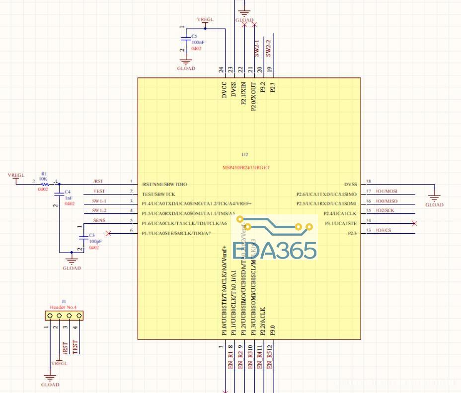
图7.开发平台FM4-U120-9B560电路图(1)
图8.开发平台FM4-U120-9B560电路图(2)
图9.开发平台FM4-U120-9B560电路图(3)
图10.开发平台FM4-U120-9B560电路图(4)
图11.开发平台FM4-U120-9B560电路图(5)
图12.开发平台FM4-U120-9B560电路图(6)
图13.开发平台FM4-U120-9B560电路图(7)
图14.开发平台FM4-U120-9B560电路图(8)
『本文转载自网络,版权归原作者所有,如有侵权请联系删除』


 热门文章
更多
热门文章
更多

 STM32中断向量表的位置.重定向


 APP下载
APP下载 登录
登录


