×


JTAG的接口是一种特殊的4/5个接脚接口连到芯片上 ,所以在电路版上的很多芯片可以将他们的JTAG接脚
通过Daisy Chain的方式连在一起,并且Probe只需连接到一个“JTAG端口”就可以访问一块印刷电路板上的所有IC。
这些连接引脚是:
TDI(测试数据输入)
TDO(测试数据输出)
TCK(测试时钟)
TMS(测试模式选择)
TRST(测试复位)可选。
因为只有一条数据线,通信协议有必要像其他串行设备接口,如SPI一样为串列传输。
时钟由TCK引脚输入。配置是通过TMS引脚采用状态机的形式一次操作一位来实现的。
每一位数据在每个TCK时钟脉冲下分别由TDI和TDO引脚传入或传出。
可以通过加载不同的命令模式来读取芯片的标识,对输入引脚采样,驱动(或悬空)输出引脚,
操控芯片功能,或者旁路(将TDI与TDO连通以在逻辑上短接多个芯片的链路)。
TCK的工作频率依芯片的不同而不同,但其通常工作在10-100MHz(每位10-100ns)。
当在集成电路中进行边界扫描时,被处理的信号是在同一块IC的不同功能模块间的,而不是不同IC之间的。
TRST引脚是一个可选的相对待测逻辑低电平有效的复位开关——通常是异步的,但有时也是同步的,依芯片而定。
如果该引脚没有定义,则待测逻辑可由同步时钟输入复位指令而复位。
尽管如此,极少消费类产品提供外部的JTAG端口接口,但作为开发样品的残留,
这些接口在印刷电路板上十分常见。在研发后,这些接口常常为反向工程提供了非常良好的途径。
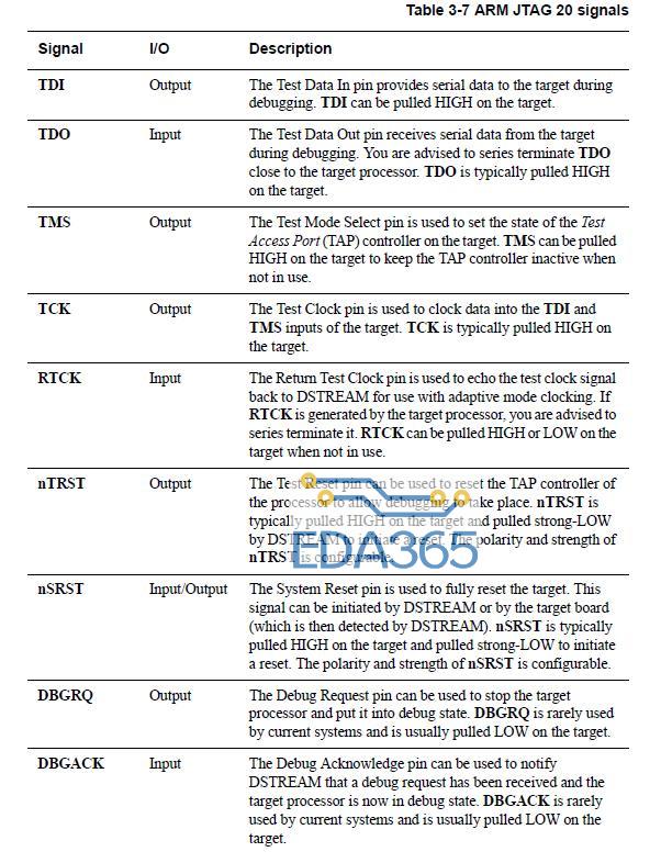
Test Clock Input (TCK)
TCK为TAP的操作提供了一个独立的、基本的时钟信号,TAP的所有操作都是通过这个时钟信号来驱动的。
Test Mode Selection Input(TMS)
TMS信号用来控制TAP状态机的转换。通过TMS信号,可以控制TAP在不同的状态间相互转换。TMS信号在TCK的上升沿有效。
Test Data Input(TDI)
TDI是数据输入的接口。所有要输入到特定寄存器的数据都是通过TDI输入端口串行输入的(由TCK驱动)。
Test Data Output(TDO)
TDO是数据输出的接口。所有要从特定的寄存器中输出的数据都是通过TDO输出端口串行输出的(由TCK驱动)。
Test Reset Input(TRST)
TRST可以用来对TAP Controller进行复位(初始化)。
不过这个信号接口在IEEE 1149.1标准里是可选的,因为通过TMS也可以对TAP Controller进行复位(初始化)操作。
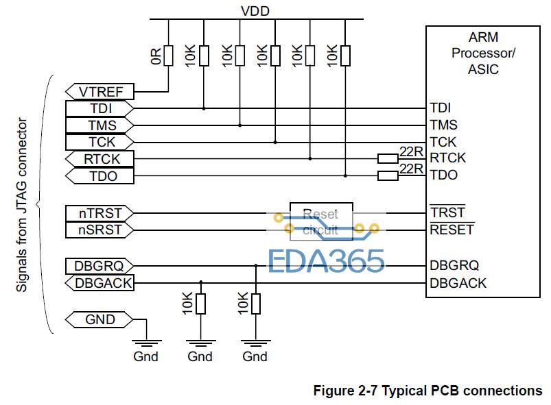
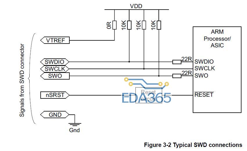
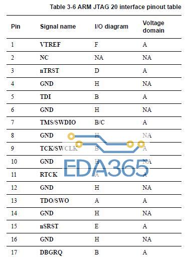
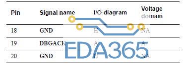
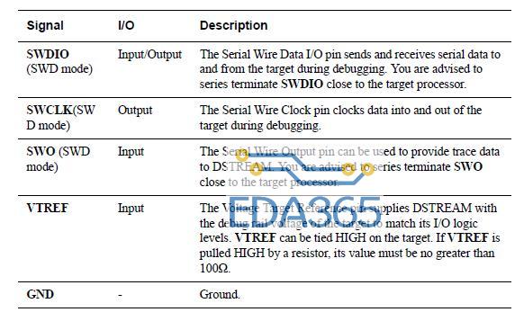
(VTREF) :接口信号电平参考电压一般直接连接Vsupply。
这个可以用来确定ARM的JTAG接口使用的逻辑电平(比如3.3V,还是5.0V)
Return Test Clock ( RTCK) :
可选项,由目标端反馈给仿真器的时钟信号,用来同步TCK信号的产生,不使用时直接接地。
System Reset ( nSRST):
可选项,与目标板上的系统复位信号相连,可以直接对目标系统复位。
同时可以检测目标系统的复位情况,为了防止误触发应在目标端加上适当的上拉电阻。
Note
• The signals TDI, TMS, TCK, RTCK and TDO are typically pulled up on the target board to keep them stable when the debug equipment is not connected.
• DBGRQ and DBGACK are typically pulled down on the target.
• If there is no RTCK signal provided on the processor, it can either be pulled to a fixed logic level or connected to the TCK signal to provide a direct loop-back.
• All pull-up and pull-down resistors must be in the range 1K-100KΩ.
• The VTREF signal is typically connected directly to the VDD rail. If a series resistor is used to protect against short-circuits, it must have a value no greater than 100Ω.
• To improve signal integrity, it is good practice to provide an impedance matching resistor on the TDO and RTCK outputs of the processor.
The value of these resistors, added to the impedance of the driver must be approximately equal to 50Ω.

In a JTAG device that fully complies to IEEE1149.1-2001, TDI and TMS are sampled on the rising edge of TCK,
and TDO changes on the falling edge of TCK.
To take advantage of these properties, DSTREAM samples TDO on the rising edge of TCK and changes its TDI and TMS signals on the falling edge of TCK.
This means that with a fully compliant target, issues with minimum setup and hold times can always be resolved by decreasing the TCK frequency,
because this increases the separation between signals changing and being sampled.
Note
There are no separate timing requirements for adaptive clocking mode,
because the minimum Tbsch and Tbscl times are identical and are the same as for non-adaptive clocking.
Tbsis and Tbsih are relative to RTCK rising, and not TCK rising, as RTCK is used to sample TDO in adaptive clocking mode.
The only real timing difference is that in adaptive mode,
DSTREAM samples TDO on the rising edge of RTCK and not TCK, so TDO timing is relative to RTCK.
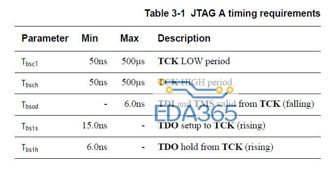
The debug software enables you to change the TCK frequency.
The TCK LOW:HIGH mark-space ratio is always 50:50.
The other parameters must be considered with the specific values of Tbscl and Tbsch that you have chosen.
The default values for an autoconfigured single-TAP system are, nominally, Tbscl=50ns and Tbsch=50ns.
• Tbsod is the maximum delay between the falling edge of TCK and valid levels on the TDI and TMS DSTREAM output signals.
The target samples these signals on the following rising edge of TCK
and so the minimum setup time for the target, relative to the rising edge of TCK, is Tbscl–Tbsod.
• Tbsis is the minimum setup time for the TDO input signal, relative to the rising edge of TCK when DSTREAM samples this signal.
The target changes its TDO value on the previous falling edge of TCK
and so the maximum time for the target TDO level to become valid, relative to the falling edge of TCK, is Tbscl–Tbsis.
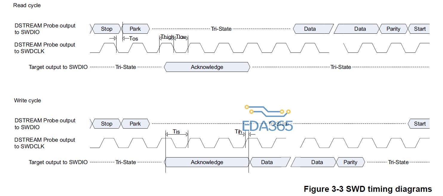
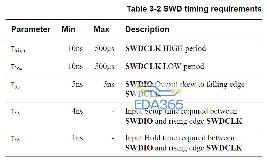
The SWDIO, SWCLK and SWO signals are typically pulled up on the target to keep them stable when the debug equipment is not connected.
• All pull-up resistors must be in the range 1K-100KΩ.
• The VTREF signal is typically connected directly to the VDD rail. If a series resistor is used to protect against short-circuits, it must have a value no greater than 100Ω.
• To improve signal integrity, it is good practice to provide an impedance matching resistor on the SWDIO and SWO outputs of the processor.
The value of these resistors, added to the impedance of the driver must be approximately equal to 50Ω.

OPEN-JTAG 开发小组
1 前言
这篇文章主要介绍 ARM JTAG 调试的基本原理。
基本的内容包括了 TAP (TEST ACCESS PORT) 和 BOUNDARY-SCAN ARCHITECTURE 的介绍,
在此基础上,结合 ARM7TDMI 详细 介绍了的 JTAG 调试原理。
这篇文章主要是总结了前段时间的一些心得体会,希望对想了解 ARM JTAG 调试的网友们 有所帮助。
我个人对 ARM JTAG 的理解还不是很透彻,在文章中,难免会有偏失和不准确的地 方,
希望精通 JTAG 调试原理的大侠们不要拍砖,有什么问题提出来,我一定尽力纠正。
同时 也欢迎对 ARM JTAG 调试感兴趣的朋友们一起交流学习。
2 IEEE Standard 1149.1 - Test Access Port and Boundary-Scan Architecture
既然是介绍 JTAG 调试,还是让我们从 IEEE 的 JTAG 调试标准开始吧。
JTAG 是 JOINT TEST ACTION GROUP 的简称。IEEE 1149.1 标准就是由 JTAG 这个组织最初提出的,最终由 IEEE 批准并且标准化的。
所以,这个 IEEE 1149.1 这个标准一般也俗称 JTAG 调试标准。
接 下 来的这 一 部分, 主 要简单 的 介绍了 TAP (TEST ACCESS PORT) 和 BOUNDARY-SCAN ARCHITECTURE 的基本构架。
虽然不是很全面,但对了解 JTAG 的基本 原理来说,应该是差不离了。
如果希望更全面深入的了解 JTAG 的工作原理,可以参考 IEEE 1149.1 标准。
2-1 边界扫描
在 JTAG 调试当中,边界扫描(Boundary-Scan)是一个很重要的概念。
边界扫描技术的 基本思想是在靠近芯片的输入输出管脚上增加一个移位寄存器单元。
因为这些移位寄存器单 元都分布在芯片的边界上(周围),所以被称为边界扫描寄存器(Boundary-Scan Register Cell)。
当芯片处于调试状态的时候,这些边界扫描寄存器可以将芯片和外围的输入输出隔离开来。
通过这些边界扫描寄存器单元,可以实现对芯片输入输出信号的观察和控制。
对于芯片的输 入管脚,可以通过与之相连的边界扫描寄存器单元把信号(数据)加载倒该管脚中去;
对于 芯片的输出管脚,也可以通过与之相连的边界扫描寄存器“捕获”(CAPTURE)该管脚上的 输出信号。
在正常的运行状态下,这些边界扫描寄存器对芯片来说是透明的,所以正常的运 行不会受到任何影响。
这样,边界扫描寄存器提供了一个便捷的方式用以观测和控制所需要 调试的芯片。
另外,芯片输入输出管脚上的边界扫描(移位)寄存器单元可以相互连接起来, 在芯片的周围形成一个边界扫描链(Boundary-Scan Chain)。
一般的芯片都会提供几条独立的 边界扫描链,用来实现完整的测试功能。
边界扫描链可以串行的输入和输出,通过相应的时 钟信号和控制信号,就可以方便的观察和控制处在调试状态下的芯片。
利用边界扫描链可以实现对芯片的输入输出进行观察和控制。
下一个问题是:如何来管 理和使用这些边界扫描链?
对边界扫描链的控制主要是通过 TAP(Test Access Port)Controller 来完成的。
在下一个小节,我们一起来看看 TAP 是如何工作的。
2-2 TAP (TEST ACCESS PORT)
在上一节,我们已经简单介绍了边界扫描链,而且也了解了一般的芯片都会提供几条边 界扫
『本文转载自网络,版权归原作者所有,如有侵权请联系删除』


 热门文章
更多
热门文章
更多

 MSP430F5529 上手小例程2


 APP下载
APP下载 登录
登录


