×


LED硬件连接如下图所示:高电平点亮LED。

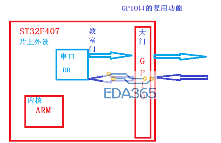
要想将PB9管脚配置成输入模式,程序所需如下步骤:(必须的)
第一步:配置系统时钟。见STM32F103x RCC寄存器配置
除此之外,还需将GPIO外设时钟打开。
/* Enable GPIOC and GPIOB clock */
RCC_APB2PeriphClockCmd(RCC_APB2Periph_GPIOB, ENABLE);
RCC_APB2PeriphClockCmd(RCC_APB2Periph_GPIOC, ENABLE);
第二步:配置中断向量表。决定将程序下载到RAM中还是FLASH中。以后讲。
void NVIC_Configuration(void)
{
#ifdef VECT_TAB_RAM
/* Set the Vector Table base location at 0x20 */
NVIC_SetVectorTable(NVIC_VectTab_RAM, 0x0);
#else /* VECT_TAB_FLASH */
/* Set the Vector Table base location at 0x08 */
NVIC_SetVectorTable(NVIC_VectTab_FLASH, 0x0);
#endif
}
第三步:配置GPIO的模式。输入模式还是输出模式。STM32_GPIO配置及库函数讲解——LED跑马灯已讲过。
void GPIO_Configuration(void)
    {
      GPIO_InitTypeDef GPIO_InitStructure;

      /* Configure PC.06, PC.07, PC.08 and PC.09 as Output push-pull */
      GPIO_InitStructure.GPIO_Pin = GPIO_Pin_6  GPIO_Pin_7  GPIO_Pin_8  GPIO_Pin_9;
      GPIO_InitStructure.GPIO_Speed = GPIO_Speed_50MHz;
      GPIO_InitStructure.GPIO_Mode = GPIO_Mode_Out_PP;
      GPIO_Init(GPIOC, &GPIO_InitStructure);

      /* Configure PB.09 as Input pull-up */
      GPIO_InitStructure.GPIO_Pin =  GPIO_Pin_9;
      GPIO_InitStructure.GPIO_Mode = GPIO_Mode_IPU;  //上拉输入
      GPIO_Init(GPIOB, &GPIO_InitStructure);
    }
第四步:读该管脚上的电平状态。需要介绍一个库函数。
v GPIO_ReadInputDataBit 从指定Port指定Pin,读该管脚上的电平状态:
u8 GPIO_ReadInputDataBit(GPIO_TypeDef* GPIOx, u16 GPIO_Pin)
{
u8 bitstatus = 0x00;
/* Check the parameters */
assert_param(IS_GPIO_ALL_PERIPH(GPIOx));
assert_param(IS_GET_GPIO_PIN(GPIO_Pin));
if ((GPIOx->IDR & GPIO_Pin) != (u32)Bit_RESET)
{
bitstatus = (u8)Bit_SET;
}
else
{
bitstatus = (u8)Bit_RESET;
}
return bitstatus;
}
涉及到GPIO_IDR寄存器,如下所示


经过上面4步,就可以检测PB9管脚的电平状态。
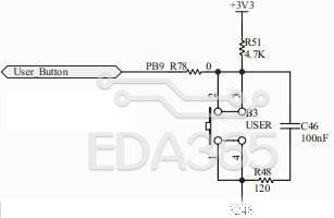
按键按下,PB9管脚应该是低电平,怎么才能验证,最简单的方法是:当按键被按下,点亮所有LED。
下面给出完整程序:
/* Includes */
#include "stm32f10x_lib.h"
/* Private function prototypes --*/
void RCC_Configuration(void);
void NVIC_Configuration(void);
void GPIO_Configuration(void);
void Delay(vu32 nCount);
/*******************************************************************************
* Function Name : main
* Description : Main program.
* Input : None
* Return : None
*******************************************************************************/
int main(void)
{
#ifdef DEBUG
debug();
#endif
/* Configure the system clocks */
RCC_Configuration();
/* NVIC Configuration */
NVIC_Configuration();
/* Configure the GPIO ports */
GPIO_Configuration();
/* Infinite loop */
while (1)
{
if (GPIO_ReadInputDataBit(GPIOB, GPIO_Pin_9) == 0) //检测USR键是否被按下,若按下,则点亮全部LED
{
GPIO_SetBits(GPIOC, GPIO_Pin_6 GPIO_Pin_7 GPIO_Pin_8 GPIO_Pin_9);
}
else
{
GPIO_ResetBits(GPIOC, GPIO_Pin_6 GPIO_Pin_7 GPIO_Pin_8 GPIO_Pin_9);
}
}
}
/*******************************************************************************
* Function Name : RCC_Configuration
* Description : Configures the different system clocks.
* Input : None
* Return : None
*******************************************************************************/
void RCC_Configuration(void)
{
ErrorStatus HSEStartUpStatus;
/* RCC system reset(for debug purpose) */
RCC_DeInit();
/* Enable HSE */
RCC_HSEConfig(RCC_HSE_ON);
/* Wait till HSE is ready */
HSEStartUpStatus = RCC_WaitForHSEStartUp();
if (HSEStartUpStatus == SUCCESS)
{
/* Enable Prefetch Buffer */
FLASH_PrefetchBufferCmd(FLASH_PrefetchBuffer_Enable);
/* Flash 2 wait state */
FLASH_SetLatency(FLASH_Latency_2);
/* HCLK = SYSCLK */
RCC_HCLKConfig(RCC_SYSCLK_Div1);
/* PCLK2 = HCLK */
RCC_PCLK2Config(RCC_HCLK_Div1);
/* PCLK1 = HCLK/2 */
RCC_PCLK1Config(RCC_HCLK_Div2);
/* PLLCLK = 8MHz * 9 = 72 MHz */
RCC_PLLConfig(RCC_PLLSource_HSE_Div1, RCC_PLLMul_9);
/* Enable PLL */
RCC_PLLCmd(ENABLE);
/* Wait till PLL is ready */
while(RCC_GetFlagStatus(RCC_FLAG_PLLRDY) == RESET) {}
/* Select PLL as system clock source */
RCC_SYSCLKConfig(RCC_SYSCLKSource_PLLCLK);
/* Wait till PLL is used as system clock source */
while(RCC_GetSYSCLKSource() != 0x08) {}
}
/* Enable GPIOC and GPIOB clock */
RCC_APB2PeriphClockCmd(RCC_APB2Periph_GPIOB, ENABLE);
RCC_APB2PeriphClockCmd(RCC_APB2Periph_GPIOC, ENABLE);
}
/*******************************************************************************
* Function Name : NVIC_Configuration
* Description : Configures Vector Table base location.
* Input : None
* Return : None
*******************************************************************************/
void NVIC_Configuration(void)
{
#ifdef VECT_TAB_RAM
/* Set the Vector Table base location at 0x20 */
NVIC_SetVectorTable(NVIC_VectTab_RAM, 0x0);
#else /* VECT_TAB_FLASH */
/* Set the Vector Table base location at 0x08 */
NVIC_SetVectorTable(NVIC_VectTab_FLASH, 0x0);
#endif
}
/*******************************************************************************
* Function Name : GPIO_Configuration
* Description : Configures the different GPIO ports.
* Input : None
* Return : None
*******************************************************************************/
void GPIO_Configuration(void)
{
GPIO_InitTypeDef GPIO_InitStructure;
/* Configure PC.06, PC.07, PC.08 and PC.09 as Output push-pull */
GPIO_InitStructure.GPIO_Pin = GPIO_Pin_6 GPIO_Pin_7 GPIO_Pin_8 GPIO_Pin_9;
GPIO_InitStructure.GPIO_Speed = GPIO_Speed_50MHz;
GPIO_InitStructure.GPIO_Mode = GPIO_Mode_Out_PP;
GPIO_Init(GPIOC, &GPIO_InitStructure);
/* Configure PB.09 as Input pull-up */
GPIO_InitStructure.GPIO_Pin = GPIO_Pin_9;
GPIO_InitStructure.GPIO_Mode = GPIO_Mode_IPU; //上拉输入
GPIO_Init(GPIOB, &GPIO_InitStructure);
}
/*******************************************************************************
* Function Name : Delay
* Description : Inserts a delay time.
* Input : nCount: specifies the delay time length.
* Return : None
*******************************************************************************/
void Delay(vu32 nCount)
{
for(; nCount != 0; nCount--);
}
#ifdef DEBUG
/*******************************************************************************
* Function Name : assert_failed
* Description : Reports the name of the source file and the source line number
* where the assert_param error has occurred.
* Input : - file: pointer to the source file name
* - line: assert_param error line source number
* Return : None
*******************************************************************************/
void assert_failed(u8* file, u32 line)
{
/* User can add his own implementation to report the file name and line number,
ex: printf("Wrong parameters value: file %s on line %d\r\n", file, line) */
/* Infinite loop */
while (1)
{
}
}
#endif
还有个问题:PB9的初始状态是什么?或者说GPIO_Configuration函数后PB9管脚上是高电平还是低电平?
这要看GPIO_InitStructure结构体的GPIO_Mode成员变量初始化为什么,如果为上拉,则PB9管脚为高电平;如果为下拉,则PB9管脚为低电平。
GPIO管脚内部电路设计如图:
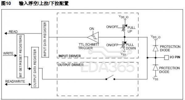
当GPIO初始化为输入上拉模式,由上图可知:该端口向外输出高电平,即:ODR对应位为1
当GPIO初始化为输入下拉模式,由上图可知:该端口向外输出低电平,即:ODR对应位为0
如何调试:在下面两处处设个断点。
1. GPIO初始化函数GPIO_Configuration中

可以看到:当GPIO设置成输入上拉模式时,等待GPIO初始化完毕,该管脚ODR9为1
2. 在main函数中,设置一个断点。
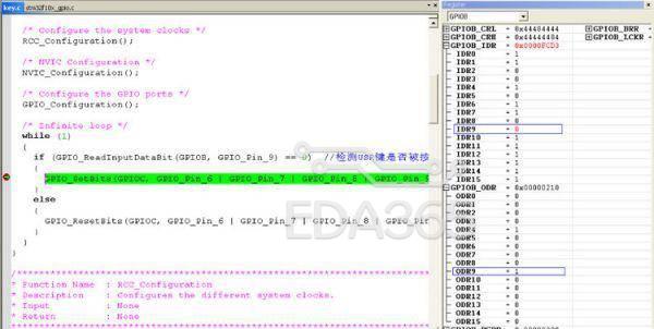
全速执行(F5),按住User Button不放,可以看到GPIOB_IDR的IDR9=0。当放开按键时,再单步调试(F10),
GPIOB_IDR的IDR9=1。
『本文转载自网络,版权归原作者所有,如有侵权请联系删除』


 热门文章
更多
热门文章
更多

 如何升级STM32单片机的代码


 APP下载
APP下载 登录
登录


