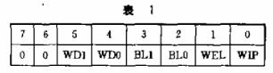
×


The Cortex-M3 and Cortex-M4 have a predefined memory map. This allows the built-in peripherals, such as the interrupt controller and the debug components, to be accessed by simple memory access instructions.
Thus, most system features are accessible in program code. The predefined memory map also allows the Cortex-M3 processor to be highly optimized for speed and ease of integration in system-on-a-chip (SoC) designs.
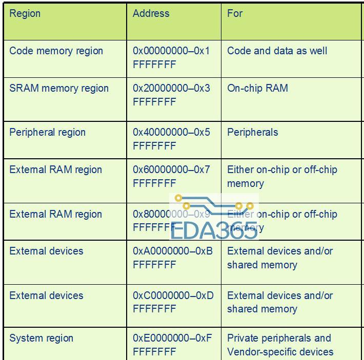
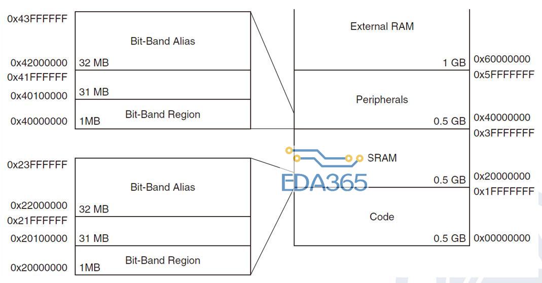
Overall, the 4 GB memory space can be divided into ranges as shown in picture below. The Cortex-M3 design has an internal bus infrastructure optimized for this memory usage.
A graphical representation of the ARM memory is shown in picture below :
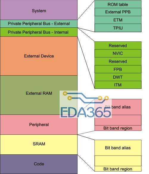
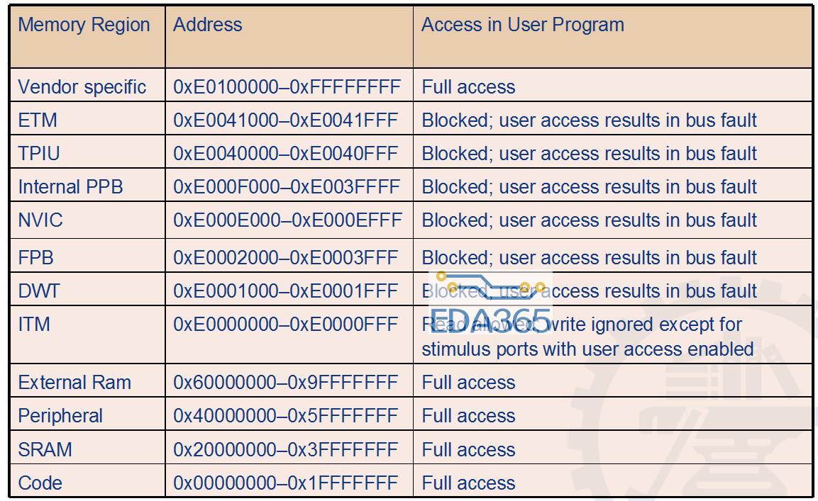
The ARM Cortex-M3 memory is divided into following regions :
System - .
Private Peripheral Bus - External - Provides access to :
the Trace Port Interface Unit (TPIU),
the Embedded Trace Macrocell (ETM),
the ROM table,
implementation-specific areas of the PPB memory map.
Private Peripheral Bus - External - Provides access to :
the Instrumentation Trace Macrocell (ITM),
the Data Watchpoint and Trace (DWT),
the Flashpatch and Breakpoint (FPB),
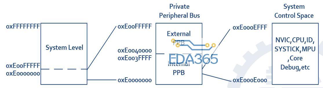
the System Control Space (SCS), including the MPU and the Nested Vectored Interrupt Controller (NVIC).
External Device - This region is used for external device memory.
External RAM - This region is used for data.
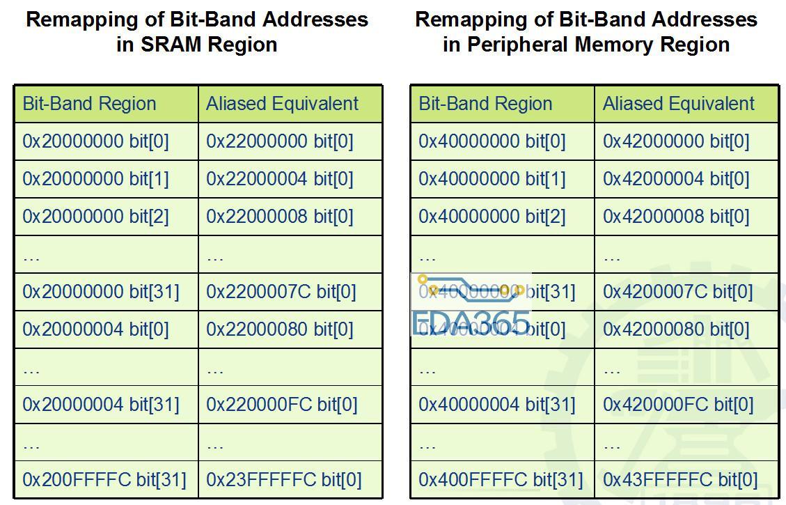
Peripheral - This region includes bit band and bit band alias areas.
Peripheral Bit-band alias - Direct accesses to this memory range behave as peripheral memory accesses, but this region is also bit addressable through bit-band alias.
Peripheral bit-band region - Data accesses to this region are remapped to bit band region. A write operation is performed as read-modify-write.
SRAM - This executable region is for data storage. Code can also be stored here. This region includes bit band and bit band alias areas.
SRAM Bit-band alias - Direct accesses to this memory range behave as SRAM memory accesses, but this region is also bit addressable through bit-band alias.
SRAM bit-band region - Data accesses to this region are remapped to bit band region. A write operation is performed as read-modify-write.
Code - This executable region is for program code. Data can also be stored here.
Memory Maps
The Cortex-M3 processor has a fixed memory map.
Some of the memory locations are allocated for private peripherals such as debugging components.
1. Fetch Patch and BreakPoint Unit (FPB)
2. Data WatchPoint and Trace Unit (DWT)
3. Instrumentation Trace Macrocell (ITM)
4. Embedded Trace Macrocell (ETM)
5. Trace Port Interface Unit (TPIU)
6. ROM Table
The Cortex-M3 processor has a total of 4 GB of address space.
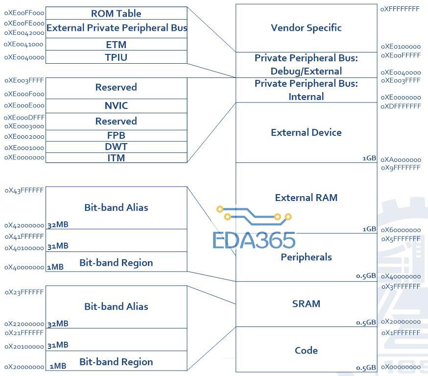
SRAM: 0.5 GB.
The SRAM memory range is for connecting internal SRAM.
On-chip peripherals: 0.5 GB
supports bit-band alias and is accessed via the system bus interface.
External RAM: 1 GB.
Program execution is allowed.
External devices: 1 GB.
Program execution is not allowed.
System-level components + internal private peripheral buses + external private peripheral bus + vendor-specific system peripherals: 0.5 GB.
Private peripheral bus:
1. AHB private peripheral bus, for Cortex-M3 internal AHB peripherals only.
2. APB private peripheral bus, for Cortex-M3 internal APB devices as well as external peripherals.
Bit-Band Operations
Bit-band operation support allows a single load/store (read/write) operation to access a single data bit.
Bit-band regions:
1. The first 1 MB of the SRAM region
2. The first 1 MB of the peripheral region
They can be accessed via a separate memory region called the bit-band alias.
To set bit 2 in word data in address 0x20000000
Write:
1. Without Bit-Band:
LDR R0, =0x20000000 ; Setup address LDR R1, [R0] ;
Read ORR.W R1, #0x4 ; Modify bit
STR R1, [R0] ; Write back result
2. With Bit-Band:
LDR R0, =0x22000008 ; Setup address
MOV R1, #1 ; Setup data
STR R1, [R0] ; Write
Read:
1. Without Bit-Band:
LDR R0, =0x20000000 ; Setup address
LDR R1, [R0] ; Read
UBFX.W R1, R1, #2, #1 ; Extract bit[2]
2. With Bit-Band:
LDR R0, =0x22000008 ; Setup address
LDR R1, [R0] ; Read
For read operations, the word is read and the chosen bit location is shifted to the LSB of the read return data.
For write operations, the written bit data is shifted to the required bit position, and a READ-MODIFY-WRITE is performed.
关键字:Cortex-M3 Cortex-M4 Memory Organization『本文转载自网络,版权归原作者所有,如有侵权请联系删除』


 热门文章
更多
热门文章
更多

 单片机中高阻态的实质及意义


 APP下载
APP下载 登录
登录


