APP下载
APP下载 登录
登录


一、摘要:
SPI 接口应用十分广泛,在很多情况下,人们会用软件模拟的方法来产生SPI 时序或是采用带SPI 功能模块的MCU。但随着可编程逻辑技术的发展,人们往往需要自己设计简单的SPI 发送模块。本文介绍一种基于FPGA 的将并行数据以SPI 串行方式自动发送出去的方法。
二、关键字:
VHDL、FPGA、SPI、串行数据输出选择模块、移位脉冲产生模块、SPI 时钟采集信号和无相移的SPI 基准时钟产生模块、SPI 时钟输出选择模块、8bit SPI 时钟采集生成模块、16bit SPI 时钟采集生成模块、24bit SPI 时钟采集生成模块、8bit 数据移位模块、16bit 数据移位模块、24bit 数据移位模块。
三、功能框图: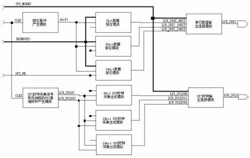
SPI_MODES 为输入模式选择端口:
--01is 8bit 传输模式
--10is 16bit 传输模式
--11is 24bit 传输模式
CLKS 为整个模块的基准时钟
DBINOUTS 为并行数据输入端口:
--8bit 模式为DBINOUTS(7 downto 0)
--16bit 模式为DBINOUTS(15 downto 0)
--24bit 模式为DBINOUTS(23 downto 0)
SPI_WR 为启动SPI 传输的信号
整个功能模块可工作在 8bit、16bit、24bit SPI 猝发传输状态。对其进行软件操作的步骤相当简单:
--此模块软件操作流程如下
--1、SPI_MODES=xx 设定串口操作模式
--2、DBINOUTS=xxxxxxxxxxxxxxxxxxxxxxxx 输入要发射的数据
--3、SPI_WR='0'
--4、SPI_WR='1'
--5、SPI_WR='0'
--8bit 模式延时2*8*4*CLKS
--16bit 模式延时2*16*4*CLKS
--24bit 模式延时2*24*4*CLKS
--6、DBINOUTS=xxxxxxxxxxxxxxxxxxxxxxxx 输入下一个要发射的数据
四、VHDL 描述解读
--以下描述的是一个SPI 自动发射模块
--在很多情况下,人们会用软件模拟的方法来产生SPI 时序
--这里采用硬件的方法,即使软件操作更为简单,有提高了传输的速度
--------------------------------------------------------------
--此模块软件操作流程如下
--1、SPI_MODES=xx 设定串口操作模式
--2、DBINOUTS=xxxxxxxxxxxxxxxxxxxxxxxx 输入要发射的数据
--3、SPI_WR='0'
--4、SPI_WR='1'
--5、SPI_WR='0'
--8bit 模式延时2*8*4*CLKS
--16bit 模式延时2*16*4*CLKS
--24bit 模式延时2*24*4*CLKS
--6、DBINOUTS=xxxxxxxxxxxxxxxxxxxxxxxx 输入下一个要发射的数据
library ieee;
use ieee.std_logic_1164.all;
use ieee.std_logic_unsigned.all;
entity SPI_interface is
port(CLKS :in std_logic; --基准时钟
LCD_SCLS :out std_logic;--SPI 发射时钟,上升沿有效
LCD_SDIS :out std_logic;--SPI 数据串行输出口
SPI_MODES :in std_logic_vector(1 downto 0);
--串口操作模式选择
--01is 8bit trans mode
--10is 16bit trans mode
--11is 24bit trans mode
SPI_WR :in std_logic; --启动串口发送信号
DBINOUTS :in std_logic_vector(23 downto 0));
--背发送数据的并行输入口
--8bit mode use DBINOUTS(7 downto 0)
--16bit mode use DBINOUTS(15 downto 0)
--24bit mode use DBINOUTS(23 downto 0)
end;
architecture SPI_interface_behav of SPI_interface is
signal DB8BIT_reg :std_logic_vector(7 downto 0); --8bit 数据移位寄存器
signal DB16BIT_reg :std_logic_vector(15 downto 0);--16bit 数据移位寄存器
signal DB24BIT_reg :std_logic_vector(23 downto 0);--24bit 数据移位寄存器
signal counter4 :std_logic_vector(3 downto 0); --移位脉冲产生计数器
signal counter4s :std_logic_vector(1 downto 0); --SPI 时钟生成计数器
signal counter8 :std_logic_vector(4 downto 0); --8bit SPI 时钟控制计数器
signal counter16 :std_logic_vector(5 downto 0); --16bit SPI 时钟控制计数器
signal counter24 :std_logic_vector(5 downto 0); --24bit SPI 时钟控制计数器
signal shift :std_logic;--移位时钟脉冲
signal LCD_SCLSS :std_logic;--SPI 时钟采集信号
signal LCD_SCLSSS :std_logic;--无相移的SPI 基准时钟
signal LCD_SCLSS8 :std_logic;--8bit SPI 时钟信号
signal LCD_SCLSS16 :std_logic;--16bit SPI 时钟信号
signal LCD_SCLSS24 :std_logic;--24bit SPI 时钟信号
signal LCD_SDIS_8BIT :std_logic;--8bit SPI 数据信号
signal LCD_SDIS_16BIT :std_logic;--16bit SPI 数据信号
signal LCD_SDIS_24BIT :std_logic;--24bit SPI 数据信号
begin
--串行数据输出选择模块
u1:process(LCD_SDIS_8BIT,LCD_SDIS_16BIT,LCD_SDIS_24BIT,SPI_MODES)
begin
if SPI_MODES=01 then --选择8bit 串行数据输出
LCD_SDIS=LCD_SDIS_8BIT;
elsif SPI_MODES=10 then --选择16bit 串行数据输出
LCD_SDIS=LCD_SDIS_16BIT;
elsif SPI_MODES=11 then --选择24bit 串行数据输出
LCD_SDIS=LCD_SDIS_24BIT;
else LCD_SDIS='1';
end if;
end process;
--移位脉冲产生模块
u2:process(CLKS)
begin
if CLKS='1' and CLKS'event then
if counter4=0011 then
counter4=0000;
shift ='1';
else counter4=counter4+1;
shift ='0';
end if;
end if;
end process;
--SPI 时钟采集信号和无相移的SPI 基准时钟产生模块
u3:process(CLKS)
begin
if CLKS='1' and CLKS'event then
if counter4s11 then
counter4s=counter4s+1;
else counter4s=00;
end if;
end if;
LCD_SCLSS=counter4s(0); --SPI 时钟采集信号
LCD_SCLSSS=counter4s(1); --无相移的SPI 基准时钟
end process;
--SPI 时钟输出选择模块
u4:process(LCD_SCLSS8,LCD_SCLSS16,LCD_SCLSS24,SPI_MODES)
begin
if SPI_MODES=01 then
LCD_SCLS=LCD_SCLSS8; --选择8bit SPI 时钟模式
elsif SPI_MODES=10 then
LCD_SCLS=LCD_SCLSS16; --选择16bit SPI 时钟模式
elsif SPI_MODES=11 then
LCD_SCLS=LCD_SCLSS24; --选择24bit SPI 时钟模式
else LCD_SCLS='1';
end if;
end process;
--8bit SPI 时钟采集生成模块
counter8_u:process(LCD_SCLSS)
begin
if SPI_WR='1' then
counter8=10001;
elsif LCD_SCLSS='1' and LCD_SCLSS'event then
if counter8>0 then
counter8=counter8-1;
LCD_SCLSS8=LCD_SCLSSS;
end if;
end if;
end process;
--16bit SPI 时钟采集生成模块
counter16_u:process(LCD_SCLSS)
begin
if SPI_WR='1' then
counter16=100001;
elsif LCD_SCLSS='1' and LCD_SCLSS'event then
if counter16>0 then
counter16=counter16-1;
LCD_SCLSS16=LCD_SCLSSS;
end if;
end if;
end process;
--24bit SPI 时钟采集生成模块
counter24_u:process(LCD_SCLSS)
begin
if SPI_WR='1' then
counter24=110011;
elsif LCD_SCLSS='1' and LCD_SCLSS'event then
if counter24>0 then
counter24=counter24-1;
if (counter24=000000)or(counter24=000001)or
(counter24=110011)or(counter24=000010)then
LCD_SCLSS24='0';
else
LCD_SCLSS24=LCD_SCLSSS;
end if;
end if;
end if;
end process;
--8bit 数据移位模块
DB8BIT_U:process(shift,SPI_WR,DBINOUTS)
begin
if SPI_WR='1' then
DB8BIT_reg=DBINOUTS(7 downto 0);
else
if shift='1' and shift'event then
LCD_SDIS_8BIT=DB8BIT_reg(0);
DB8BIT_reg(6 downto 0)=DB8BIT_reg(7 downto 1);
end if;
end if;
end process;
--16bit 数据移位模块
DB16BIT_U:process(shift,SPI_WR,DBINOUTS)
begin
if SPI_WR='1' then
DB16BIT_reg(15 downto 0)=DBINOUTS(15 downto 0);
else
if shift='1' and shift'event then
LCD_SDIS_16BIT=DB16BIT_reg(0);
DB16BIT_reg(14 downto 0)=DB16BIT_reg(15 downto 1);
end if;
end if;
end process;
--24bit 数据移位模块
DB24BIT_U:process(shift,SPI_WR,DBINOUTS)
begin
if SPI_WR='1' then
DB24BIT_reg(23 downto 0)=DBINOUTS(23 downto 0);
else
if shift='1' and shift'event then
LCD_SDIS_24BIT=DB24BIT_reg(0);
DB24BIT_reg(22 downto 0)=DB24BIT_reg(23 downto 1);
end if;
end if;
end process;
end;
五、仿真波形图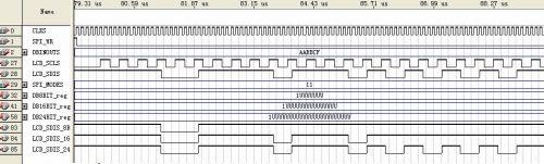
六、编译后资源占用情况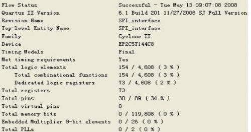
七、结束语
本文旨在给学习可编程技术的人们提供一个参考,起到抛砖引玉的作用。望阅读过此文的读者提供更好的方法,与所有的学习者共享,共勉!


 热门文章
热门文章